Thin-Film Solar Cells
Collaboration
The collaboration formed between Mines and NREL through Ryan O’Hayre and David Ginley establishes a rich environment for research and learning. The resources available through both institutions allow for cutting edge thin film solar research. One project that is currently sponsored through this collaboration is the development and processing of metal organic decomposition precursors for CIS solar cells.
Importance of Thin Film Solar Research
Most of the world’s energy comes from fossil fuels, including coal, natural gas, and petroleum. These resources, however plentiful, are not unlimited, and are not without environmental impact [1, 2]. According to the National Renewable Energy Laboratory’s report to the U.S. Department of Energy, approximately 140 million acres of land in the U.S. is covered with cities and residences. If only 7% of this area were slated for dual-use with commercially available photovoltaics, the entire Nation’s electricity requirements could be supplied [3]. Dual-use areas can include rooftops, siding on buildings and skyscrapers, parking lots, and various other sites. It is important to note that once greater than 10% of the Nation’s total energy is generated via photovoltaics, integral storage would have to be implemented.
Additionally, fossil fuel prices have experienced significant volatility over the last several years, a trend that is not likely to disappear in the near future [4]. At the same time, the market for solar energy in the US is expected to grow exponentially over the next decade [5]. As a forward-thinking society, the US must utilize science to produce viable, renewable, alternative energy sources. Thin-film solar cells are excellent candidates because they use a renewable energy (solar radiation) to produce electricity without any air pollution. The long-term benefits of such technology are wide spread and include both environmental and health impacts [1, 2, 6, 7].
Thin film CIS solar cells have demonstrated efficiencies greater than 19% [8, 9], butto date they have not made a significant impact on the overall energy market.This is primarily because the current processing approaches used to produce CIS solar cells employ physical vapor deposition in ultra high vacuum chambers and/or highly toxic gases like H2Se.These approaches have proven difficult to scale to large area and high throughput production. Additionally, the use of either vacuum technology [7, 10, 11]or dangerous gases increases the processing costs significantly and does not allow CIS cells to be cost-competitive with other energy alternatives, specifically fossil fuels [7,12]. The processing approach used in this project eliminates the need for vacuum chamber deposition and the use of toxic gases.Additionally, the processing technique may be easily integrated into a flow-through manufacturing process and it minimizes the difficulties with the volatility of Se. This will significantly reduce the overall costs of cell production and make CIS solar cells a more viable and cost-effective option [7].
Research Objectives
Metal organic decomposition (MOD) inks were fabricated for deposition, processing, and characterization in this project. Indium-selenide (In-Se), copper-selenide (Cu-Se), and copper indium diselenide (CIS) films were produced and characterized. The main objective is to understand the mechanisms of phase transformation that drive the MOD ink derived precursor films to produce In-Se films, Cu-Se films, and CIS films. The secondary objective is to understand how deposition and processing affect film composition, morphology, and phase formation. These objectives are addressed through multiple studies, each a portion of the research conducted for this project.
CIS Basics
The structural properties of CIS depend on the composition of the overall compound. The chemical formula for CIS is CuInSe2, making it part of the Cu-chalcogenide family. The most common structure for stoichiometric CuInSe2 is therefore the tetragonal chalcopyrite structure shown in Figure 1. This structure corresponds with the space group characterized by tetrahedral coordination of each lattice site to its nearest neighbors.As can be seen in Figure 1, two copper and two indium cations surround each Se anion [1, 2, 13, 14]. This arises from the composition of CIS and the pseudo-binary phase diagram for the Cu2Se-In2Se3 system (Figure 2) where the chalcopyrite structure is represented by a.
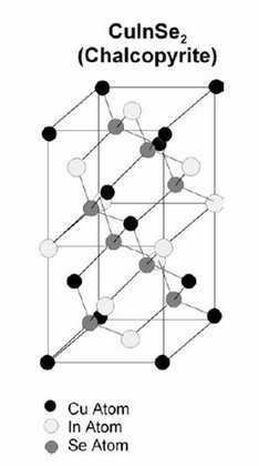
Figure 1. CulnSe2 Chalcopyrite Structure [14].
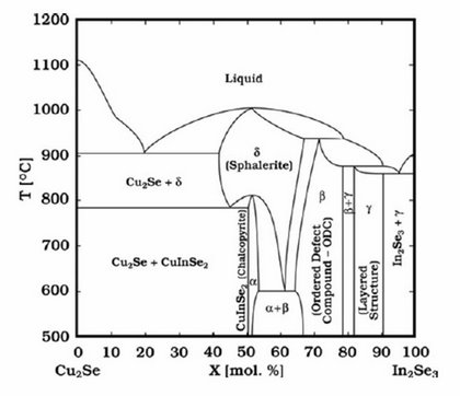
Figure 2. Pseudo-Binary Phase Diagram for the Cu2Se-In2Se3system [13-15].
CIS solar cells consist of a layered structure, shown in Figure 3. The bottom layer is the substrate, usually soda lime glass. This is coated with a back contact layer of molybdenum, approximately 1 µm thick. The CIS absorber layer is then deposited (via one of several methods discussed in a later section), and is between 2 and 3 µm thick. Next, a 50 nm thick CdS junction-forming layer is grown by chemical bath deposition (also discussed in a later section). After that, radio-frequency sputtering (RF-sputtering) is used to deposit first a layer of undoped ZnO (~50 nm thick) and then a doped, conducting ZnO layer (~200 to 300 nm thick). ZnO is used because it is a transparent conducting oxide (TCO) and forms a window layer.On top of the TCO layer, a nickel/aluminum current collection gird and an anti-reflection coating of MgF2 (~100nm thick) are deposited via separate electron beam (e-beam) evaporation steps. Finally, for testing purposes the cell undergoes mechanical scribing or photolithographic patterning to define the active area. This is not necessary in industrial applications [16, 17].
Figure 3. Structure of the CIS Solar Cell [18].
References
- Kemell, M., M. Ritala, and M. Leskela, Thin film deposition methods for CulnSe(2) solar cells. Critical Reviews in Solid State and Materials Sciences, 2005. 30(1): p. 1-31.
- AbuShama, J.A.M., Investigation of Cu-In-Ga-Se Thin Film Growth Dynamics for High Efficiency Solar Cells, in Physics. 2003, Colorado School of Mines: Golden. p. 205.
- PV FAQs: How Much Land Will PV Need to Supply Our Electricity. 2003, National Renewable Energy Laboratory: Golden. p. 1-2.
- Awerbuch, S., Determining the real cost: Why renewable power is more cost-competitive then previously believed, in Renewable Energy World. 2003.
- Sharp sets up 20MW solar module assembly in Memphis, Tennessee.Photovoltaics Bulletin, 2003. 2003(1): p. 1-2.
- Drewes, P., Now for something different � spheral solar technology.Photovoltaics Bulletin, 2003. 2003(1): p. 8-9.
- Ginley, D., et al., Inkjet Direct-Write Solar Cells. 2005, National Renewable Energy Laboratory: Golden. p. 1-46.
- Schock, H.W. and R. Noufi, CIGS-based solar cells for the next millennium. Progress in Photovoltaics, 2000. 8(1): p. 151-160.
- Ramanathan, K., et al., Properties of 19.2% efficiency ZnO/CdS/CuInGaSe2 thin-film solar cells. Progress in Photovoltaics, 2003. 11(4): p. 225-230.
- Eberspacher, C., et al., Thin-film CIS alloy PV materials fabricated using non-vacuum, particles-based techniques. Thin Solid Films, 2001. 387(1-2): p. 18-22.
- Altosaar, M., et al., Further developments in CIS monograin layer solar cells technology. Solar Energy Materials and Solar Cells, 2005. 87(1-4): p. 25-32.
- Kazmerski, L. and T. Surek, Anyone else for TFT? Photovoltaics Bulletin, 2003. 2003(1): p. 3.
- Stanbery, B.J., Copper indium selenides and related materials for photovoltaic devices. Critical Reviews in Solid State and Materials Sciences, 2002. 27(2): p. 73-117.
- Rudmann, D., Effects of Sodium on Growthh and Properties of Cu(In,Ga)Se2 Thin Films and Solar Cells, in Department of Physics. 2004, Swiss Federal Institute of Technology: Zurich.
- Anderson, T., Processing of CuInSe2-Based Solar Cells: Characterization of Deposition Processes in Terms of Chemical Reaction Analyses. 1999, University of Florida: Gainesville, FL. p. 1-56.
- Ginley, D., et al., Direct-Write Optoelectronics: Combining Nanoscale Material Science and Inkjet Printing to Produce Novel Optoelectronic Materials and Devices. 2004, National Renewable Energy Laboratory: Golden. p. 1-7.
- Probst, V., et al., Rapid CIS-process for high efficiency PV-modules: development towards large area processing. Thin Solid Films, 2001. 387(1-2): p. 262-267.
- Contreras, M., et al. High Efficiency Cu(In,Ga)Se2-Based Solar Cells: Processing of Novel Absorber Structures. in 24th PVSC IEEE. 1994. Hawaii.